I like to think I can learn something about our readers from the list of most read semiconductor articles. What I think I’ve learned from this year’s list is that you are as obsessed as I am with packing more and more computing power into less and less space. That’s good, because it’s the main goal of a huge chunk of the industry as well.
Not all of this list fits neatly into that mold, but hey, who doesn’t love a millimeter-scale laser chip that can slice through steel?
1971 was a special year for a number of reasons—the first e-book was posted, the first one-day international cricket match was played, this reporter was born. It was also the first time the semiconductor industry sold more than 1 trillion transistors. If TSMC executives’ predictions are correct, there will be 1 trillion transistors in just one GPU within a decade. Just how the foundry plans to deliver such a technological feat was the subject of the most read semiconductor story we posted this year.

Susumu Noda
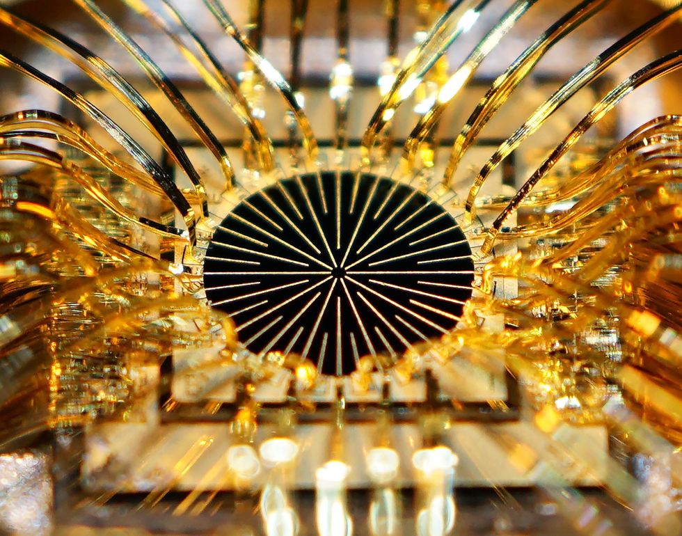
Slicing through steel and other feats of optical superheroism have, until very recently, been the reserve of large carbon dioxide lasers and similarly bulky systems. But now, centimeter-scale semiconductors have joined the club. Called photonic crystal semiconductor lasers (PCSELs), the devices take advantage of a complex array of carefully shaped nanometer-scale holes inside the semiconductor to steer more energy straight out of the laser. A PCSEL built in Japan produced a steel-slicing beam that diverges just 0.5 degrees.
Intel had some big ambitions at the beginning of the year. Things are looking a lot less rosy now. Nevertheless, the predictions of this January 2024 issue article have come to pass. Intel is set to manufacture chips using a combination of two new technologies, nanosheet transistors and back side power delivery. Although the main competition, TSMC, is moving to nanosheets soon, too, the foundry behemoth is leaving back side power for later. But Intel’s plans didn’t completely survive contact with customers and competition. Instead of commercializing its first iteration of the combo, called 20A, it’s skipping on to the next version, called 18A.

Chris McKenney/Georgia Institute of Technology
Graphene has long been an interesting material for future electronics but a frustrating one, too. Electrons zip through it at speeds silicon could only wish for, tempting researchers with the potential of terahertz transistors. But it has no natural bandgap, and it’s proven really difficult to give it one. But Georgia Tech researchers have given it one more go and come up with a pretty straightforward way to make a semiconductor version atop a wafer of silicon carbide.

Intel
Intel’s foundry division is pinning its hopes on gaining foundry customers for its 18A process, which, as noted above, combines nanosheet transistors and back side power delivery. There haven’t been a lot of details about what customers plan to build with this tech, but Intel executives did explain to IEEE Spectrum how they planned to use those technologies, and some advanced packaging too, in a server CPU codenamed Clearwater Forest.
 David Plunkert
Can anyone beat Nvidia? It’s the subtext of so many articles about AI hardware, that we thought we should ask it explicitly. The answer: A very solid maybe. It all depends on what you’re trying to beat the company at.

iStock
In a year when the United States inked a blitz of preliminary deals as part of its $52-billion attempt to reinvigorate its chipmaking industry, our loyal readers were way more interested in India’s somewhat smaller moves. That government announced a trio of deals, including the country’s first silicon CMOS fab. A key architect of India’s plans to boost chip R&D explained it all to IEEE Spectrum later in the year.
 imec
imec
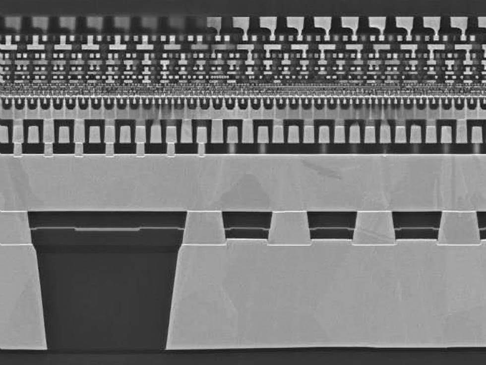
Chip packaging is one of the most important aspects of the continuation of Moore’s Law, enabling systems made of many different silicon dies linked together as if they were one gigantic chip. And the hottest thing in advanced packaging is a technology called 3D hybrid bonding. (I know this because I sat in on no less than 20 talks about it at the IEEE Electronic Components Technology Conference in May 2024.) 3D hybrid bonding joins chips together in a vertical stack with connections so dense you could fit millions of them in a square millimeter.
 KEK
KEK
Just when you thought the making of advanced chips was already a bonkers process, here comes a hint that the future will be even more bananas than the present. Extreme-ultraviolet lithography today relies on a Rube-Goldberg-esque procedure of zapping flying droplets of molten tin with kilowatt-class lasers to produce glowing balls of plasma. But future chipmaking will want brighter light than such a system could provide. The answer, some say, is a gigantic particle accelerator that saves energy by using the high-energy physics version of regenerative braking.

Tesla
Like cowbell in a certain 1970s rock anthem, future computers need more silicon. How much? How about a whole wafer’s full of it. Back in April, the world’s biggest foundry, TSMC, laid out its plans for advanced packaging, and that future points toward wafer-scale computers. TSMC has technically been making one for a while now for Cerebras, but what it’s planning to offer in the coming years will be much more flexible and universally available. In 2027 the technology could lead to systems with 40 times as much computing power as today’s
From Your Site Articles
Related Articles Around the Web

